Semiconductor Strain Gauges
Model: SYP series
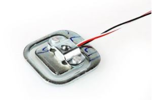
Description
Semiconductor Strain Gauges: Overview and Applications
Semiconductor strain gauges leverage the piezoresistive properties of materials like silicon or germanium to measure strain. Unlike traditional metallic foil gauges, they offer significantly higher sensitivity but come with trade-offs in linearity and temperature stability.
Comparison to Metallic Foil Gauges
| Feature | Semiconductor Gauges | Metallic Foil Gauges |
|---|---|---|
| Sensitivity | Very High | Low-Moderate |
| Temperature Stability | Poor (requires compensation) | Good |
| Linearity | Moderate (nonlinear at high strain) | Excellent |
| Durability | Fragile | Robust |
| Cost | High | Low |
Features
- High Sensitivity: Ideal for detecting tiny deformations (e.g., in MEMS devices or biomedical sensors).
- Miniaturization: Can be fabricated at microscale for integration into compact systems (e.g., pressure sensors in smartphones).
- Fast Response: Suitable for high-frequency dynamic measurements.
- Low Power Consumption: Useful in battery-operated devices.
Technical Data
Semiconductor strain gauge characteristics
|
Model Number |
SYP-15 |
SYP-30 |
SYP-60 |
SYP-120 |
SYP-350 |
SYP-600 |
SYP-1000 |
|
Gage resistance(Ω) |
15±5% |
30±5% |
60±5% |
120±5% |
350±5% |
600±5% |
1000±5% |
|
Code |
B,C |
B,C |
B,C |
A,B,C |
B,C |
C |
C,D |
|
construction |
0,F2,F3,F4,F5 |
0,F2,F3,F4,F5 |
0,F2,F3,F4,F5 |
0,F2,F3,F4,F5 |
0,F2,F3,F4,F5 |
0,F2,F3,F4,F5 |
C:0,F2,F3,F4,F5 |
|
K |
100 |
100 |
120 |
A:150 |
150 |
200 |
C:200 |
|
TCR (%/℃) |
0.10 |
0.10 |
0.15 |
0.13 |
0.30 |
0.45 |
C:0.40 |
|
TCGF (%/℃) |
-0.12 |
-0.12 |
-0.18 |
A:-0.35 |
-0.35 |
-0.48 |
C:-0.48 |
|
maximum operating current(mA) |
50 |
50 |
50 |
A:20 |
30 |
20 |
20 |
|
Strain limits(mε) |
5000 |
5000 |
5000 |
5000 |
5000 |
5000 |
5000 |
Dimension
|
Semiconductor strain gauge (without substrate) |
|||
|
Code |
configuration |
size (mm) |
Gage resistance |
|
A |
|
1.27×0.22×(0.020~0.030) |
15Ω,30Ω,60Ω,120Ω |
|
B |
|
3.8×0.22×(0.020~0.030) |
15Ω,30Ω,60Ω,120Ω,350Ω |
|
C |
 |
4.7×0.22×0.02 |
15Ω,30Ω,60Ω,120Ω,350Ω,600Ω,1000Ω |
|
D |
|
6×0.22×0.02 |
1000Ω |
|
① The copper wire length of Semiconductor strain gage (without substrate) is shorter than 6mm; |
|||


Example: SYP 1000 C F3
explicate: P-Si Semiconductor strain gage
resistance: 1000Ω;
K: 200;
Silicon: 4.7×0.22×0.02;
Substrate size: 7×4.
Applications:
- Nonlinear compensation of foil sensor
- Machinery aviation ships bridges
- Micro pressure sensor
Note: if there are other requirements or the size of the substrate or the silicon strip must be specified in the contract
Hot Tags: Semiconductor Strain Gauges, China, manufacturers, suppliers, factory, made in China